Samsung Cuts HBM Development Time to One Year, Focusing on Securing NVIDIA Orders
Samsung Electronics has officially decided to significantly shorten the research and development cycle for High Bandwidth Memory (HBM) from approximately two years to within one year. Samsung has a plan to launch a new generation of HBM annually, aligning with the release pace of new AI accelerators from major customers like NVIDIA.
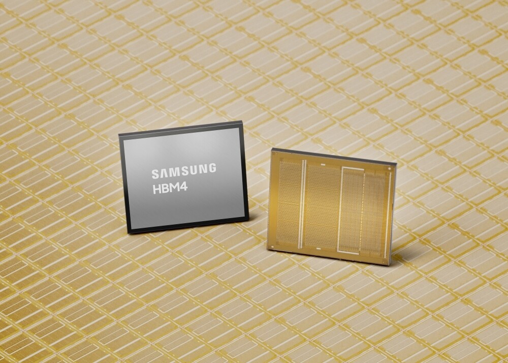
HBM is a core component of AI accelerators. Samsung's latest mass-produced product is HBM3E, and the next-generation HBM4 is expected to launch this year alongside NVIDIA's Vera Rubin and AMD's Instinct MI400 platforms.
In March of this year, Samsung publicly showcased a physical sample of HBM4E at NVIDIA GTC 2026, achieving a transfer rate of 16Gbps and a bandwidth of 4.0TB/s. The first batch of HBM4E samples has been scheduled for production in May 2026 and will be prioritized for NVIDIA's evaluation.
However, AI accelerator manufacturers have generally shifted to a product release cycle of updating one generation per year. HBM suppliers that cannot keep pace risk technological lag and even customer loss.
More urgently, market research firm Counterpoint data shows that SK Hynix is expected to account for approximately 54% of the global HBM market share in 2026, while Samsung accounts for only about 28%.
Samsung's proactive compression of the R&D cycle is essentially aligning the supply chain rhythm with customer roadmaps, embedding itself in the core chain of the AI hardware ecosystem.
Samsung Memory Product & Technology Executive Vice President SangJoon Hwang revealed at GTC 2026 that the base die for HBM5 will be upgraded from a 4nm process to a 2nm process across generations.