ASML: Memory Chip EUV Orders Surpass Logic Chip Orders for the First Time
Driven by strong demand for both logic and memory chips, ASML is increasing its investment in AI-driven infrastructure. ASML states that the supply of advanced logic and memory chips will remain constrained in the foreseeable future.
During the Q1 2026 earnings call, ASML President and CEO Christophe Fouqet emphasized that with the expansion of AI factories to the next stage, demand for advanced logic and memory chips is growing exponentially, and the company is increasing investment in the necessary tools to accelerate the production of advanced logic and memory chips in the AI ecosystem.
Customers are actively increasing production capacity, driven by capacity constraints in end markets including artificial intelligence, mobile devices, and personal computers.
The company announced Q1 2026 sales by system, with 51% of market share coming from memory-related end application systems and the remaining 49% of sales from logic design. EUV lithography remains dominant, accounting for 66% of revenue, while DUV lithography (ArF immersion) accounts for 23% of revenue.
South Korean semiconductor factories are the busiest region globally, accounting for 45%, followed by Taiwan (23%) and mainland China (19%). The United States ranks fourth with a 12% share (Q1 2026). ASML’s majority of EUV/DUV system supply goes to Samsung, TSMC, SMIC, and Intel. ASML is currently restricted from selling its high-end EUV lithography equipment to mainland China, but sales of DUV equipment are unrestricted. However, this may change as U.S. lawmakers plan to ban exports of DUV technology to mainland China.
ASML President and CEO Christophe Fouqet stated: “Looking ahead to the market, the growth outlook for the semiconductor industry remains robust, primarily driven by investment in AI-related infrastructure. These investments are driving increased demand for advanced logic and memory chips across many areas. Demand will continue to outstrip supply in the foreseeable future. This will create supply tightness in end markets from artificial intelligence to mobile devices and personal computers, and will prompt our customers to actively expand production capacity.”
Demand in the memory sector is also growing steadily for cutting-edge EUV and DUV lithography machines as DRAM manufacturers transition to newer process nodes. ASML’s order intake continues to increase, and the company says it is working with partners to meet their needs while providing “productivity upgrades” to optimize production efficiency in the short term.
The growth in memory chip demand is primarily from HBM manufacturers such as SK Hynix, Samsung, and Micron, who rely on EUV lithography to manufacture next-generation standard chips such as HBM3E, HBM4, and HBM4E. These new standards are critical to upcoming accelerators from NVIDIA and AMD, which will be in high demand.
The ASML President and CEO emphasized that in addition to expanding capacity, the continued adoption of EUV and immersion deep ultraviolet lithography by advanced DRAM and logic device customers on new process nodes further increases their demand for lithography technology. As a result, ASML’s order intake remains strong, and we are working closely with customers to meet their needs. At the same time, we also provide customers with capacity upgrade solutions for existing equipment to meet their short-term production needs.
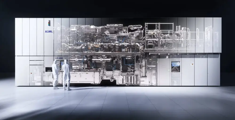
Looking ahead, ASML is committed to developing upgraded low NA EUV lithography machines with a throughput of at least 330 wafers per hour. The system is expected to be delivered in the early next decade. ASML also released a new NXE:3800E PEP-E lithography machine, increasing wafer throughput from 220 per hour to 230 per hour with similar overlay accuracy.
ASML stated that in terms of technology, we continue to make significant progress and highlighted several recent achievements at the SPIE Advanced Lithography and Patterning conference held in San Jose in February. At the conference, we released an updated low NA EUV product roadmap, reflecting improvements to our plans for these products in the short and long term. This includes achieving a throughput of at least 330 wafers per hour for low NA EUV in the early next decade, primarily due to our continued improvements in source power, as demonstrated by our recent demonstration of a 1000W source.
According to ASML’s roadmap, the company expects to launch its advanced NXE:4200G low NA system in 2029-2030, with a wafer output capacity of at least 300W/hour. At the same time, a high NA EVU system will launch the EXE:5200D, providing chips below the 2nm node (A14 and below), with a wafer output capacity of at least 175W/hour.
ASML plans to increase its chip production by 50% by the beginning of the next decade by increasing the power of the sources in its equipment by 66%. While this will not be achieved until 2030, the company is working to address supply constraints by increasing wafer throughput through upgrades to existing and upcoming equipment.