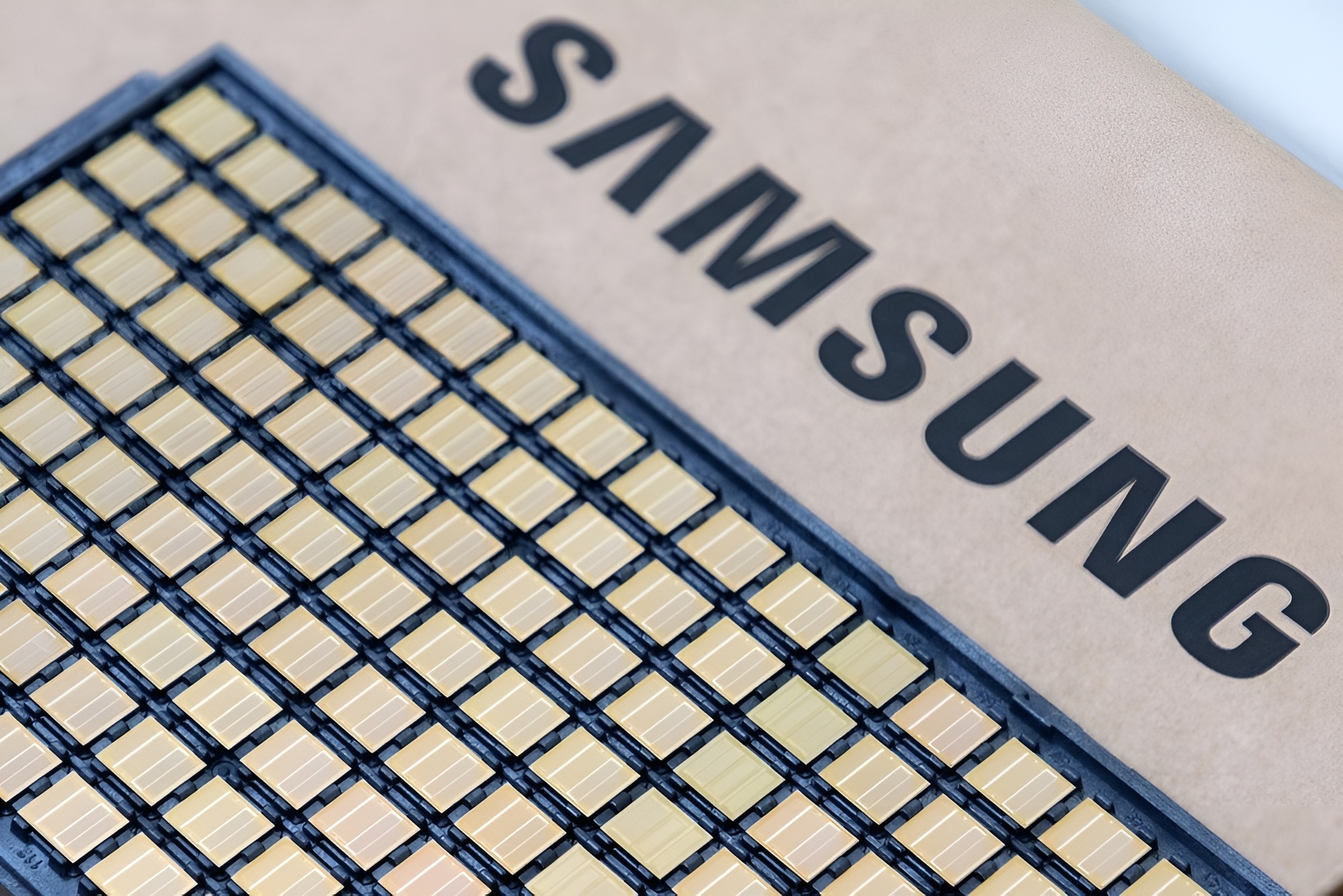
Overtaking SK Hynix Dream Shattered: Samsung Rushes into High-End Memory but Stumbles on Basic Yield Rate
Samsung's pursuit in the high-end memory sector has suffered a major setback. Due to the yield rate of key foundational technology D1dDRAM failing to reach internal targets, Samsung has decided to indefinitely postpone the mass production plan for the next-generation HBM5E memory. The problematic D1dDRAM is Samsung's seventh-generation 10nm-class process, originally intended as the core foundation for future HBM solutions, and was planned to be used in the ninth-generation HBM product, HBM5E.
Although the technology had previously received pre-production approval, the consistently low yield rate has made the return on investment for trial runs problematic, let alone mass production.
According to sources familiar with Samsung's internal affairs, Samsung plans to restart mass production only after the D1d yield reaches the target level. Currently, there is no definite timeline for recovery, and Samsung is comprehensively re-examining its process roadmap in an attempt to further improve yield rates.
Notably, Samsung's existing 1c DRAM technology is currently being stably used in its third-generation HBM products, including HBM4, HBM4E, and HBM5.
HBM4 is expected to launch later this year. NVIDIA's Vera Rubin and AMD's MI400 platforms will both adopt HBM4, and HBM4E is expected to be used in Rubin Ultra and MI500 accelerators.
Further down the line, HBM5 and custom designs are expected to be adopted by solutions such as NVIDIA's Feynman series.
Samsung has been reported to be significantly shortening the HBM development cycle, with new solutions being prepared at an unprecedented speed. However, faster development does not necessarily translate to direct mass production, and the production cycle is now the biggest bottleneck.
At the same time, Samsung is also increasing its production capacity, having invested additional resources in building a large chip factory in Uiwang, Korea, equivalent in size to four football fields, specifically for the production of next-generation DRAM products including HBM. The factory will be responsible for key links such as packaging, testing, logistics, and quality control.
Samsung's long-time rival, SK Hynix, has already completed the research and development of D1d DRAM technology and secured the yield rate.
Both companies are currently competing for large orders from leading AI companies. Whoever can make their HBM planning more flexible, while ensuring yield rates and stable investment returns, and achieve continuous research and production, will ultimately have the last laugh.