Samsung's 1dnm DRAM Yields Fall Short, Potentially Delaying HBM5E Mass Production
Recent sources reveal that Samsung's DRAM chips based on the 1dnm process (7th generation 10nm-level process) are experiencing lower-than-expected yields during trial production. Samsung has planned to indefinitely postpone mass production until the yield rate reaches its target. To this end, Samsung may comprehensively review the process flow to further improve yields.
Originally, Samsung planned to use DRAM chips manufactured with the 1dnm process for HBM5E, the ninth-generation HBM solution.
Notably, in addition to HBM4, DRAM chips using the 1cnm process will also be used for HBM4E and HBM5, covering three consecutive generations of HBM products. There are also rumors that Samsung may upgrade the base die of the next generation of HBM, switching to the more advanced 2nm process.
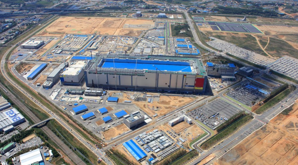
Currently, Samsung has invested more resources in 1dnm process DRAM chips and is building a new factory in South Korea.
It is reported that the factory covers an area of approximately four standard football fields and will handle packaging, testing, logistics, and quality control in addition to DRAM chip production. These processes are crucial for maintaining stable production.