Samsung Breaks Physical Limits of DRAM with First Global Production of 4F² Architecture
Samsung Electronics has successfully produced DRAM working wafers based on the 4F² architecture for the first time globally, overcoming the long-standing physical scaling limitations of conventional planar DRAM. The company first publicly showcased a 16GbDRAM prototype incorporating the 4F² architecture at the ISSCC2026 conference in February.
Samsung completed wafer production using the 10a process in March and confirmed normal chip operation through characteristic testing. This achievement marks the first global practice of integrating 4F² cell structure with Vertical Channel Transistor (VCT) technology.
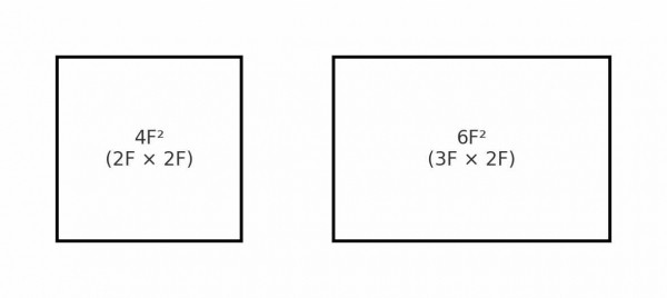
Technically, the 4F² architecture reduces the cell area of traditional DRAM from 6F² to a 2F×2F square structure, theoretically increasing unit area capacity by 30% to 50% while maintaining advantages in speed and power consumption.
To achieve this structure, Samsung introduced VCT technology, vertically erecting the transistor channel to increase channel length within a limited chip area, effectively alleviating the short-channel effect and leakage problems encountered by conventional planar transistors during scaling.
On the other hand, Samsung adopted inter-wafer hybrid copper bonding technology, separating the storage cell array and peripheral circuits for manufacturing on different wafers before vertically stacking them, achieving ultra-high-density interconnection.
The channel material was also changed from traditional silicon to indium gallium zinc oxide (IGZO) to suppress leakage current in the miniaturized cell.
In the future, more cells can be packed into the same size DRAM chip, and terminal devices such as laptops and smartphones are expected to obtain larger memory capacity and faster data throughput under the premise of small size and low power consumption.
Samsung has planned a clear roadmap – completing 10a DRAM development in 2026, conducting quality testing in 2027, and transitioning to mass production in 2028.
SK Hynix plans to introduce 4F²+VCT at the 10b node, while Micron will maintain its existing design route, and Chinese manufacturers are directly deploying 3D DRAM due to EUV restrictions.