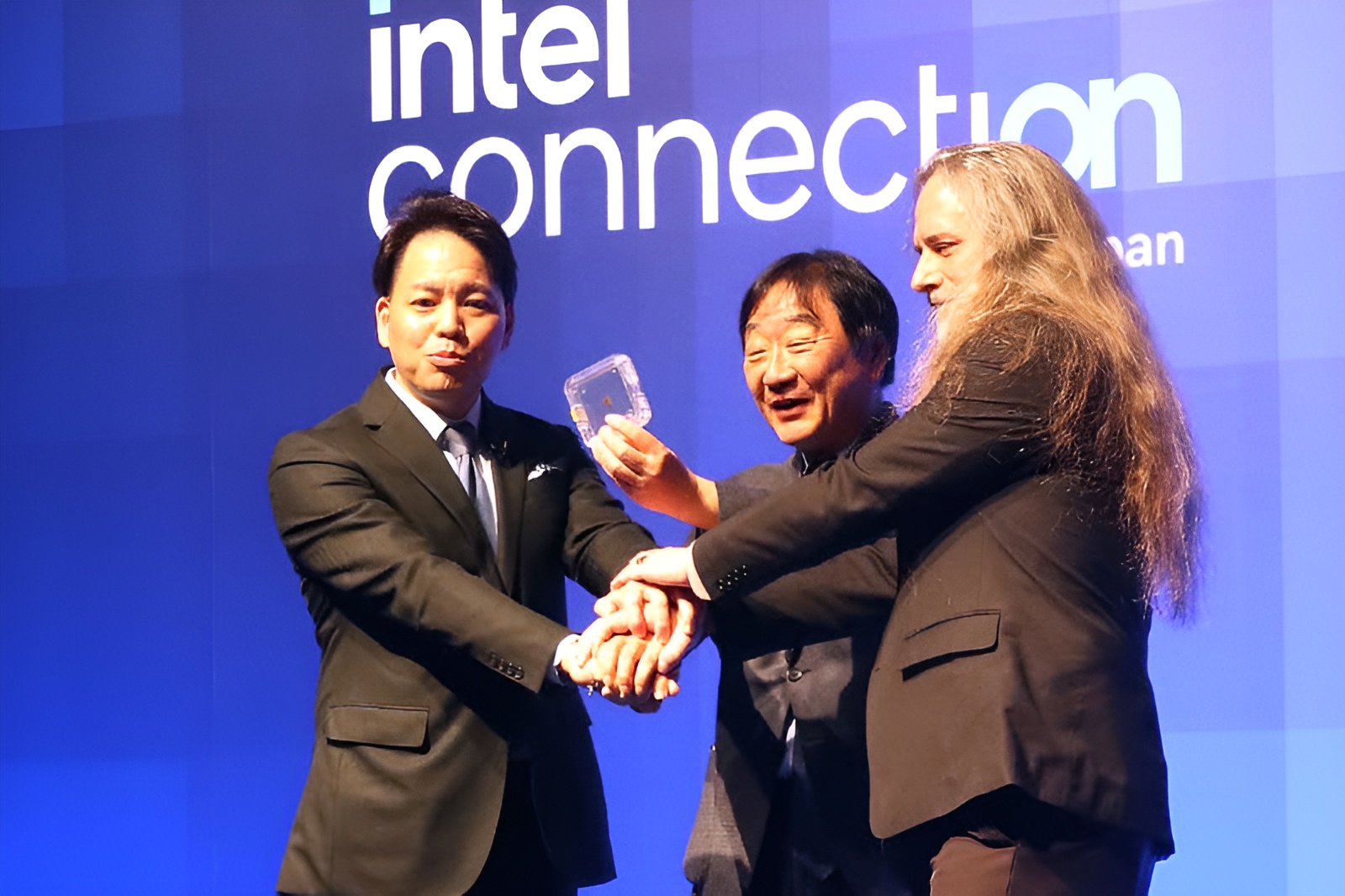
Intel and SoftBank Collaborate to Advance Next-Generation ZAM Storage, with Japanese Government Funding Accelerating Commercialization
Intel has announced that its joint project with SoftBank subsidiary SAIMEMORY, the Z-AngleMemory (ZAM) next-generation storage project, has been officially selected and funded by the New Energy and Industrial Technology Development Organization (NEDO) of Japan, accelerating the R&D process through government subsidies.
ZAM is seen as a potential alternative to High Bandwidth Memory (HBM), aiming to address storage shortages in the AI and High-Performance Computing (HPC) fields while achieving higher bandwidth, larger capacity, and significantly reduced power consumption.
According to the latest information released by Intel K.K. and SAIMEMORY, the ZAM project has been included in NEDO’s funding plan. The project is planned for approximately 3.5 years and will focus on developing a next-generation stacked DRAM architecture for the AI era. This architecture, named Z-Angle Memory, aims to provide a new memory form factor for data centers and AI acceleration scenarios under the increasingly stringent constraints of power consumption and thermal design. NEDO’s funding will help accelerate the project’s pace in areas such as technological breakthroughs, manufacturing verification, and supply chain construction, to move towards large-scale commercialization faster.
Intel stated that the company has been validating the underlying science and engineering paths related to ZAM for many years, including collaborative experiments at national laboratories under the U.S. Department of Energy, and technical exploration in the “Next-Generation DRAM Bonding Program.” Makoto Ohno, President of Intel Japan, pointed out that obtaining NEDO funding will help push these early accumulations towards faster global deployment, while further consolidating the crucial US-Japan technology partnership in the coming years.
In terms of technical approach, ZAM (Z-Angle Memory) targets core indicators including a 40%–50% reduction in power consumption compared to existing solutions, a simpler and more manufacturable stacked design, and an ultra-high capacity density of up to 512GB per chip. Specifically, ZAM adopts multi-layer tightly stacked DRAM chips, each layer connected through a so-called Z-Angle interconnect structure, and connected to the main computing chip via EMIB (Embedded Multi-die Interconnect Bridge) under the base chip to enhance bandwidth and compress power consumption and packaging complexity.
Under the new development plan, ZAM will not only be led by Intel and SAIMEMORY in R&D, but will also widely introduce technology, manufacturing, and supply chain partners from within Japan and internationally, to jointly support its advancement in design, mass production, and ecosystem building. The project aims to address the increasingly prominent memory bandwidth and capacity bottlenecks in the current AI and HPC markets, while providing a more scalable and energy-efficient storage solution for future generations of platforms.
It is worth noting that the launch of ZAM also means that Intel will officially return to the memory market with its own products after decades. In the early stages of the company’s development, Intel was an important participant in the global memory industry, but was eventually squeezed out of the dominant position by Japanese manufacturers. Today, it is the participation and support of Japanese companies and institutions that are helping Intel bring this new generation of memory technology to reality, which is historically significant.