IMEC Believes Chip Technology Can Continue for Another 20 Years, Reaching Below 0.2nm by 2046
Moore's Law, which has driven the development of global chip technology for over 50 years, has recently been declared dead by many in the industry, who believe that chip technology is approaching its physical limits and can no longer be miniaturized. However, the Belgian research center IMEC is not so pessimistic. Their recently released roadmap shows that current silicon-based technology can continue for many years, and reaching below 0.2nm by 2046 is still feasible.
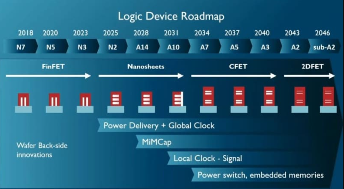
According to their published roadmap, the industry achieved N7 process at the 7nm level in 2018, and up to the N3 process at 3nm can still be achieved using FinFET transistors. Last year, the N2 process at the 2nm node began to shift to GAA transistors, using the NanoSheets route, which can continue to be used up to the A14 process at 1.4nm level and the A10 process at 1.0nm level, reaching 2031.
It is expected to enter the A7 process at 0.7nm level in 2034. At this point, GAA transistor structures will no longer work, and CFFET transistor structures will be adopted. This is a complementary field-effect transistor that vertically stacks N and P transistors, theoretically reducing the area by half, but the heat dissipation challenge is very difficult.
CFET transistors will continue to be used until the A3 process at 0.3nm level in 2040. After that, the transistor structure will have to be changed again, this time using the long-rumored 2DFET, entering the era of two-dimensional crystals, which is considered the ultimate material for chip technology, with perfect atomic-level thickness. Companies such as TSMC, Samsung, and Intel have all demonstrated this black technology, but there is still no timetable for mass production.
2DFET transistor structures can drive chip technology all the way to Sub-A2, which is below 0.2nm, and should be 0.14nm according to current naming conventions. However, it is still too early. IMEC is only proposing a PPT goal, and even the name is hard to say, after all, there are still 20 years to go.
In short, IMEC has provided a chip technology roadmap for the next 20 years, but after entering the angstrom level, each generation of process improvement is very difficult.
If you have been following TSMC's processes after 2nm, the shrinkage of chip area is no longer obvious, and it is difficult to increase density by even 10%, so many non-standard process generations have been introduced. At a recent technical forum, processes A13 and A12 were even announced, filling the gap between A14 and A10. The A11 process later on will not be surprising.
In addition, the upgrade of chip technology is not only determined by the size of the nm number, but also faces extremely high technical challenges in heat dissipation, power supply, and packaging. Whoever can solve these problems may stand out in the process competition in the next 20 years, and it is not impossible to surpass TSMC, Samsung, or Intel.
I hope that in the next 20 years of competition, Chinese companies such as SMIC, HuaHong, JHICC, and Silian Integrated can also participate, and no longer be followers.